

Super-resolution microscopy leverages digital display technology
Open source core technology built into the projector hardware enables high-speed, automatic polarization modulated 3D structured illumination microscopy (SIM) imaging. ...

Open source core technology built into the projector hardware enables high-speed, automatic polarization modulated 3D structured illumination microscopy (SIM) imaging. ...

American chipmaker Nvidia briefly surpassed Amazon in market value on Monday, as hopes for artificial intelligence pushed the chipmaker to ...
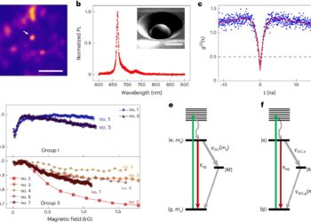
Optical properties of GaN defects. A, PL image of an isolated defect (n°2), indicated by an arrow, and its surroundings. ...
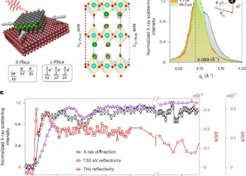
Photoinduced structural change and insulator-metal transition. A, Top left, schematic representation of a thin film strained by epitaxy (O, red; ...
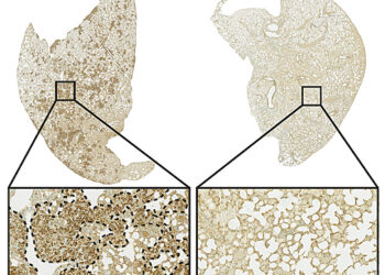
Credit: Molecular cancer (2024). DOI: 10.1186/s12943-023-01914-8 Over the past two decades, immunotherapy – which uses the body's immune system to ...

The increase in productivity of advanced stone tools (shown in white lines) did not occur before or at the start ...
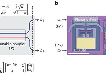
A MEMS-based 2 × 2 unitary gate and its measured responses. a, b, Schematic (a) and optical microscopy image (b) ...

The giant American technology company, Apple, succeeded in overcoming a year-long decline in sales, announcing net profits of about $34 ...

A new compact, lensless facial recognition system scans a bust of Michelangelo's David and reconstructs the image using less energy ...

An atomic-scale rendering of the Mott insulator (green) and underlying material (blue) that proved essential for refining and stabilizing the ...