
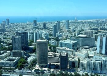
Silicon Valley wealthy people have a fortune of 15 times the money of its population economy
The French newspaper Le Monde revealed - in a recent report - an unprecedented increase in the concentration of wealth ...

The French newspaper Le Monde revealed - in a recent report - an unprecedented increase in the concentration of wealth ...
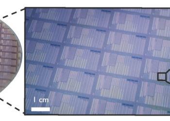
Imec, a research and innovation hub in the field of nanoelectronics and digital technologies, announced an important milestone in the ...
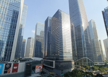
Shenzhen, southern China - The Guangdong Province in southern China, known to many Arab, Asian, African and European traders, has ...

A team of engineers, chemists and materials scientists at Stanford University has discovered that applying a short-duration voltage to certain ...
The occupation army began its brutal war against the residents of the Gaza Strip about a year ago. During this ...
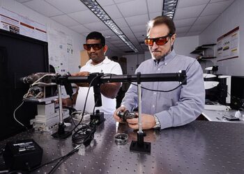
When Valery Levitas left Europe in 1999, he brought a rotating diamond anvil cell with him to the United States. ...

Research from UC Irvine reveals that the optical properties of materials can be dramatically improved, not by changing the materials ...
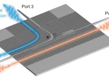
A team of scientists has harnessed the potential of 6G communications with a new polarization multiplexer. Terahertz communications represent the ...

Silicon Valley's right-wing figures, long isolated in this particularly Democratic region of California, are now uniting around Donald Trump. And ...
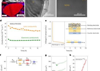
High-performance batteries are needed for a wide range of applications and demand is growing rapidly. Therefore, the research and development ...