
China announces the discovery of quantities of quartz that is important to produce semiconductors and solar panels economy
China has declared the discovery of new deposits of purity, a metal with a fundamental role in the production of ...

China has declared the discovery of new deposits of purity, a metal with a fundamental role in the production of ...

Conventional silicon-based electronics are approaching their limits in terms of performance and scalability. In recent years, engineers have therefore attempted ...

Diamond, often celebrated for its unrivaled hardness and transparency, has become an exceptional material for high-power electronics and next-generation quantum ...
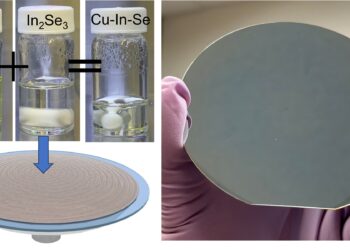
Standard manufacturing techniques for semiconductor devices (the technologies that make electronics possible) involve processing raw materials at high temperatures in ...
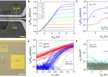
Two-dimensional (2D) semiconductor materials exhibit distinct optoelectronic properties that could be advantageous for the development of ultrathin and tunable electronic ...

Silicon Valley in California and the Silicon Slopes in Utah are named for the thing most associated with semiconductors, the ...
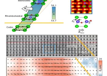
In the field of materials science, the phenomena of polarization and polarity are traditionally associated with insulators. However, let's imagine ...

A research team comprising NIMS, the University of Tokyo and the Tokyo University of Science has developed the world's first ...
Today, petrochemical compounds and rare metals such as platinum and iridium are used to produce semiconductors for optoelectronics, such as ...