Quantum annealing and the future of prime factorization
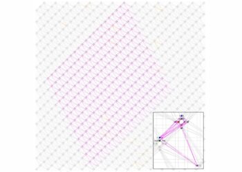
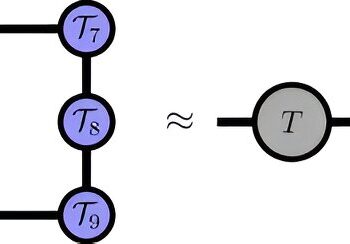
Researchers at the University of Trento, Italy, have developed a new approach to prime factorization via quantum annealing, exploiting a ...

Researchers at the University of Trento, Italy, have developed a new approach to prime factorization via quantum annealing, exploiting a ...

While atomic clocks are already the most precise time measuring devices in the universe, physicists are working hard to further ...

According to a recent study from the University of Helsinki, published in the journal Physical Examination LettersA vortex of a ...

The colored centers of diamond are the subject of an increasing number of studies due to their potential for the ...
A recent study revealed a significant advance toward on-chip integration of single-photon sources at room temperature. This achievement represents a ...
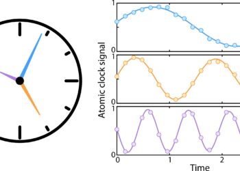
Atomic clocks are a class of clocks that exploit the resonant frequencies of atoms to tell time with great precision. ...
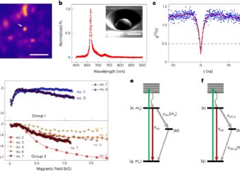
In diamonds (and other semiconductor materials), defects are the quantum sensor's best friend. Indeed, the defects, essentially an arrangement of ...
Quantum computing has been hailed as a technology capable of surpassing classical computing in speed and memory usage, potentially paving ...
A new fusion of materials, each with particular electrical properties, has all the components required for a unique type of ...
Research into quantum computing and quantum networks is underway around the world in hopes of developing a quantum internet in ...