Engineering quantum entanglement at the nanoscale
Physicists have spent more than a century measuring and understanding the strange ways that photons, electrons, and other subatomic particles ...

Physicists have spent more than a century measuring and understanding the strange ways that photons, electrons, and other subatomic particles ...

A classic way to image nanoscale structures in cells is to use expensive, high-powered super-resolution microscopes. As an alternative, MIT ...
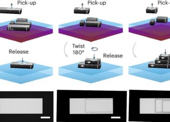
Next-generation technologies, such as advanced memory storage solutions and brain-inspired neuromorphic computing systems, could touch almost every aspect of our ...
For the first time ever, researchers observed, in real time and at the molecular scale, hydrogen and oxygen atoms fusing ...

Using nanoscale devices as small as human cells, researchers can create materials with revolutionary properties that enable smaller, faster, and ...
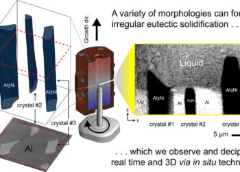
During eutectic solidification, a mixture of two or more solids self-assembles, forming composite microstructures ranging from ordered layers to complex, ...

As an innovative concept in materials science and engineering, the inspiration for self-healing materials comes from living organisms that have ...
Scientists at the University of California, Irvine, have discovered a one-dimensional nanoscale material that changes color as the temperature changes. ...

Long-standing challenges in biomedical research, such as monitoring brain chemistry and tracking the spread of drugs in the body, require ...

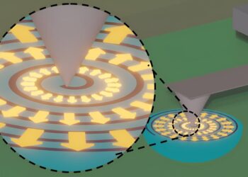
Traditional microelectronic architectures, with transistors to control electrical currents along wires, power everything from advanced computers to everyday devices. But ...