Advances in silicon photonics pave the way for cost-effective, high-performance optical devices
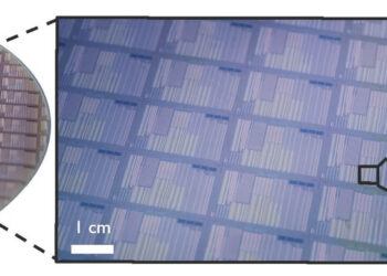
Imec, a research and innovation hub in the field of nanoelectronics and digital technologies, announced an important milestone in the ...

Imec, a research and innovation hub in the field of nanoelectronics and digital technologies, announced an important milestone in the ...

New research from the University of Pittsburgh shows that state and federal funding for abandoned mine drainage in Pennsylvania is ...
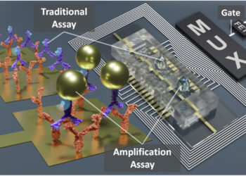
The ability to detect diseases at an early stage, or even predict their onset, would be of immense benefit to ...
A revolutionary technology has been developed that enables the production of green hydrogen in a more cost-effective and environmentally friendly ...

A new study led by the Menzies School of Health Research has provided more information on the cost-effectiveness of a ...