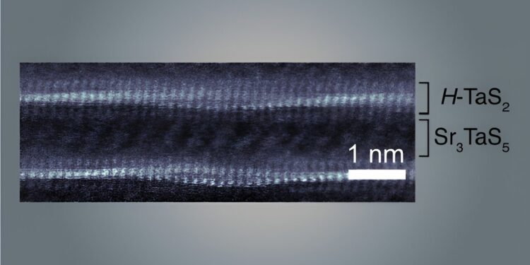
Transmission electron micrograph of a new material with wavy atomic layers. Credit: Checkelsky Lab, MIT
MIT physicists and their colleagues have created a new material with unusual superconducting and metallic properties by endlessly repeating wavy layers of atoms a few billionths of a meter thick to create a macroscopic sample that can be handled by hand. The sample’s large size makes it much easier to explore its quantum behavior, or the atomic-scale interactions that give rise to its properties.
The work, reported in Natureis also important because the material was synthesized through rational design. In other words, the recipe for the material is based on the team’s knowledge of materials science and the chemistry of this family of materials. The physicists are therefore confident that they can create even more new materials with unusual properties.
Additionally, while there are other materials that form wavy atomic structures, the team believes this is the most perfect. The nanoscopic layers of waves are uniform across an entire crystal, which is made up of thousands of these wavy layers.
“Such materials go beyond what one might traditionally think of as a crystal: observing and understanding what new physical properties might emerge is an exciting opportunity,” says Joseph Checkelsky, principal investigator of the work and an associate professor of physics at MIT.
2D Materials
Two-dimensional materials, or those made up of just one or a few layers of atoms, have attracted the attention of physicists because they can be manipulated to produce materials with new and unusual properties. For example, rotating or twisting one or more layers at a slight angle creates a unique pattern called a moiré superlattice that can give rise to phenomena such as superconductivity and unconventional magnetism.
But moiré materials are both difficult to make (they must be assembled by hand) and difficult to study because of their atomic dimensions. Checkelsky’s group set out to create analogous materials that are much easier to manipulate.
“We’re basically mixing powders of materials, exposing them to temperatures of a few hundred degrees Celsius in an oven, and relying on chemical reactions” to naturally form macroscopic crystals whose properties are dictated by interactions at the atomic level. “That’s the key breakthrough,” says Aravind Devarakonda, a Ph.D. at MIT who is now an assistant professor at Columbia University. Devarakonda is first author of the current paper. Nature paper.
In 2020, Checkelsky and several colleagues in the current work reported the first such material created this way in the journal ScienceThis article was accompanied by a perspective article by Professor Leslie M. Schoop of Princeton University.
In 2021, Checkelsky and colleagues described in Nature physics that explains how this particular material can exhibit two different types of superconductivity. The new wavy material is the second member of this family of compounds.
Like a layer cake
Like a layer cake, the new material is composed of an atomically thin metallic layer of tantalum and sulfur layered on top of a “spacer” layer of strontium, tantalum and sulfur. This structure is repeated over thousands of layers to create a large crystal.
Devarakonda and his colleagues believe that the waves form because of a mismatch between the size and structure of the crystal lattice of each layer. Similarly, one layer, made of tantalum and sulfur, bends to fit the other, forming the wave. Imagine placing a sheet of plain paper on top of a sheet of plain printer paper. For the plain paper to fit the plain paper, part of the paper would have to bend upward. The new structure is similar, except that the plain paper is “pinned” to the plain paper at regular intervals, forming waves.
Unusual goods
These tiny waves are the source of the material’s interesting properties. For example, at a certain temperature, the material can become superconductive, meaning that electrons pass through it without resistance.
In this case, “the electrons are marked by the structural modulations (waves),” Devarakonda explains. In other words, “superconductivity also picks up this ripple. In some parts it is strong, and in others it is weakened.”
Likewise, the material exhibits unusual metallic properties. Indeed, electrons find it much easier to flow into the troughs of a wave (or into a valley) rather than up and over the hills of a wave.
“So we gave the electrons directionality. It’s easier for them to flow in one direction than the other,” Devarakonda says. “We showed that by introducing (wave) structure, we can radically change the behavior of the layers. We’ve planted the flag; now we and others can launch applications. By standing on the shoulders of giants, we’ve created a whole new family of materials. It’s completely uncharted territory that has brought unexpected results, and surprises are always fun.”
In addition to Devarakonda and Checkelsky, the authors of the paper are Alan Chen, a graduate student in MIT’s Department of Electrical Engineering and Computer Science; Shiang Fang, a former postdoctoral researcher in MIT’s Department of Physics, now at Google Deepmind; David Graf of the National High Magnetic Field Laboratory; Markus Kriener of the RIKEN Center for Emergent Matter Science in Japan; Austin J. Akey of Harvard University; David C. Bell of Harvard; and Takehito Suzuki of Toho University.
More information:
A. Devarakonda et al, Evidence for banded electronic phases in a structurally modulated superlattice, Nature (2024). DOI: 10.1038/s41586-024-07589-5
Provided by Materials Research Laboratory, Massachusetts Institute of Technology
Quote:New material with wavy layers of atoms exhibits unusual superconducting properties (2024, September 19) retrieved September 20, 2024 from
This document is subject to copyright. Apart from any fair dealing for the purpose of private study or research, no part may be reproduced without written permission. The content is provided for informational purposes only.


