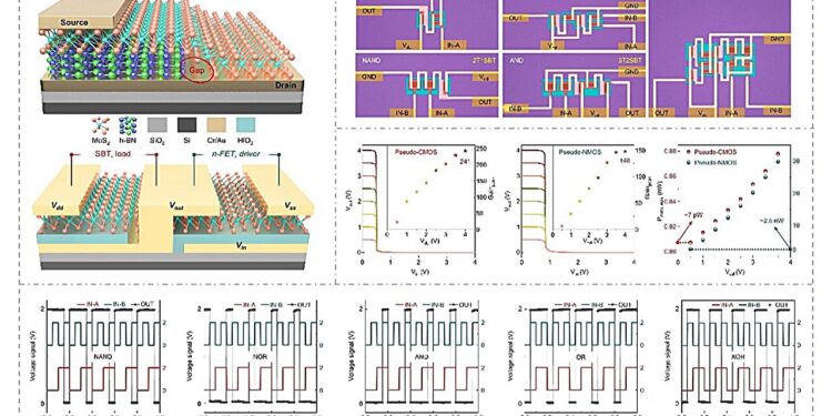
Schematic diagram, optical image and fundamental performance of logic devices based on pseudo-CMOS architecture. Credit: Wei et al.
Continuous improvement of electronic circuits and components is vital for the development of new technologies with improved capabilities and unique characteristics. In recent years, most electronics engineers have focused specifically on reducing the size of transistors, while maintaining low power consumption.
Researchers at Beijing University of Science and Technology recently introduced a new pseudo-CMOS architecture based on self-biased molybdenum disulfide transistors. This architecture, described in Natural electronicscould be used to create high-performance inverters, gate circuits, and other device components.
“The development of integrated circuits (ICs) for efficient low-power computing is a global hot topic and a focus of international competition in cutting-edge fields,” said Zheng Zhang, co-author of the paper, at Tech Xplore.
“Two-dimensional (2D) materials, such as single-layer molybdenum disulfide (MoS2), have stable structures that can exceed the physical limit of downscaling dimensions, excellent field effect properties and immunity to short channel effects, making them one of the most popular channel materials more promising for low-power integrated circuits.
Despite their advantageous structure, 2D materials aligned with conventional silicon-based circuit designs (i.e. CMOS and NMOS) have significant limitations. Specifically, the limited polarity control of their atomically thin structure poses challenges to realizing their potential in transistor design.
Zhang and his colleagues set out to design an alternative pseudo-CMOS architecture for ultra-low-power logic computing using 2D materials. Their hope was to open new avenues for the development of future ICs.
“Our pseudo-CMOS logic devices are implemented by connecting self-biased transistors (SBTs) as the load and n-type field-effect transistors (n-FETs) as the driver in series,” explained Zhang. “The homogeneous SBT with a gap barrier can timely cut off the current path (less than 1 pA) of the device when the n-FET is turned on, thereby achieving picowatt-level static power, which is only about 1% and 0.3% of the CMOS and NMOS logic device, respectively.”
By combining transistor logic (PTL) designs, the new architecture introduced by the researchers was found to reduce the number of transistors in circuits by 80% compared to conventional integrated circuit architectures. Unlike previously introduced 2D CMOS and NMOS material-based electronics, the team’s architecture bypasses the polarity control of transistors, thereby significantly reducing their static power.
“The implementation of general Boolean functions (i.e. XOR, AND, OR, NAND, NOR and NOT gates) based on a pseudo-CMOS architecture opens a scalable path towards low-power integrated circuits based on 2D materials,” Zhang said. “Our results resolve the major challenge that 2D materials cannot effectively contain the rapidly increasing static power due to limited polarity control technology.”
The architecture introduced by Zhang and colleagues could serve as inspiration for other research groups, potentially leading to the creation of new electronics with low power consumption and fast operating speeds. The researchers have already used their design to prototype inverters and gate circuits for sub-picowatt logic computing, both of which have achieved very promising results.
“In future work, we plan to develop large-scale integrated circuits of this technology, including various complex combined circuits and sequential circuits based on pseudo-CMOS architecture,” Zhang added. “This could enable the implementation of virtually all digital integrated circuits to promote the industrial application of 2D materials.”
More information:
Xiaofu Wei et al, Homojunction-charged inverters based on self-biased molybdenum disulfide transistors for sub-picowatt computing, Natural electronics (2024). DOI: 10.1038/s41928-023-01112-w
© 2024 Science X Network
Quote: An architecture for sub-picowatt logic computing based on self-biased molybdenum disulfide transistors (February 20, 2024) retrieved February 20, 2024 from
This document is subject to copyright. Apart from fair use for private study or research purposes, no part may be reproduced without written permission. The content is provided for information only.


