

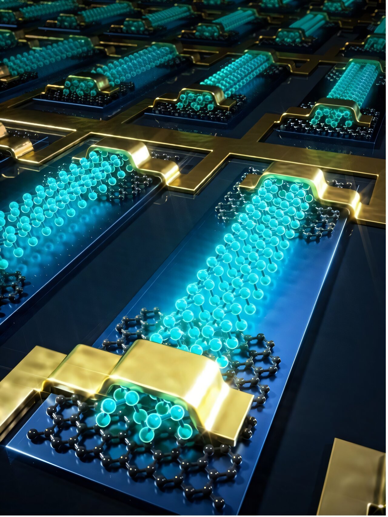
3D scientific illustration of an integrated circuit based on transistors with black nanoribbon field effects contacted with graphene. Credit: Changxin Chen Group, School of Integrated Circuits, Shanghai Jiao Tong University.
Nanoribbons with black phosphorus (BPNR), thin and narrow strips in the shape of a black phosphorus tape, are known to present very advantageous electronic properties, including an accident -tightening band. This essentially means that the energy difference between the region where the electrons are linked together (that is to say the valence strip) and that where the electrons move freely (that is to say the conduction strip) can be easily controlled by adjusting the width of nanoribbons.
An adjustable prohibited strip is essential for the development of transistors, the components which control the flow of electric current through electronic devices.
Although several previous studies have highlighted the promise of BPNRs for the development of electronics, the strategies that could allow their reliable large -scale manufacturing has yet to be lacking.
Researchers from the University of Shanghai Jiao Tong and other institutes have recently introduced a new evolutionary strategy for the realization of high quality BPNR which are consistent, have well -defined edges and present minimum defects.
Their proposed approach, described in an article published in Nature materialsBased on a technique designed to burst the materials in layers by taking advantage of ultrasonic sound waves in liquids.
“Our research group has long been devoted to the identification of ideal channel materials to allow high -performance field transistors with reduced energy and energy consumption,” said Professor Changxin Chen, who led research to Phys.org.
“BPNRs offer advantages as channel materials on other candidates such as carbon nanotubes, graphene nanoribbons and two-dimensional black phosphorus (2D) (BP). For example, BPNRs are entirely semi-controlled, unlike carbon nanotubes, which can be semiconductor or metal.
“In addition, the BPNRs have a higher compromise between mobility and the prohibited strip that graphene nanoribbons. BPNR also avoid the need to prepare crafts with large region, with a few layers, providing large -scale and largely tuning Arands.”
For some time, Chen and his colleagues have tried to design an evolutionary strategy to carry out high -quality and narrow BPNRs which have smooth edges and well -defined orientations. The manufacturing strategy introduced in their recent article is based on a newly introduced soundochemical exfoliation technique.
“We first used a short -term transport reaction to synthesize bulk BP crystals with a slightly wide -wide network parameter along the chair management,” said Chen.
“This constraint allows the crystal to decompress preferentially along the crystal plane perpendicular to the direction of the chair rather than other planes. Then, we applied appropriate ultrasonic conditions to diszip the BP in bulk crystals, thus giving high quality BPNR (1D).”
With their newly designed strategy, researchers have created nanoribbons with a width centered at 32 Nm which can be as close as 1.5 nm; The closest among the BPNRs reported to date. Remarkably, their manufacturing method presented a yield of up to 95%.
In addition, the narrow width and the zigzag edges of the resulting BPNR gave birth to a large prohibited strip, while their almost atomically smooth edges eliminated the diffusion of the carriers and led to high mobility.
“We have reached narrow and narrow BPNRs with almost atomically smooth edges and a well -defined edge orientation of high efficiency by the sound exfoliation of bulk BP crystals synthesized with a slightly widened network parameter along the chair direction,” said Chen.
“With prepared BPNR, the performance of the field transistor with an ON / OFF ratio of 1.7 × 10⁶ and mobility of 1,506 cm2 V-1 s-1Representing the highest full performance among FET based on BPNR or BP 2D bp reported so far. “”
As part of their study, Chen and his colleagues have shown that the BPNR they created could also serve as almost infrared photodeters. In fact, the narrow structures had an responsiveness of 11.2 A / W and a specific detectivity of 1.1 × 10¹¹ Cm hz1/2 W-1outperforming most of the nearby infrared detectors based on 1D nanomaterials, 2D nanomaterials and other hybrid structures.
In the future, the new manufacturing approach designed by this research team could be improved more and deployed in real contexts, allowing large -scale high -quality BPNR production. This could in turn pave the way for the development of compact electronic and optoelectronic devices which are much smaller than those available today.
“As part of our future research, we will develop controlled strategies to produce high quality COPDs with unidirectional alignment and uniform widths,” added Chen.
“Such strategies are crucial to overcome the current challenges of scalability and structural variability of BPNRs and will ultimately allow BPNR to be reliably integrated into large -scale integrated circuits.”
Written for you by our author Ingrid Fadelli, edited by Sadie Harley, and verified and revised by Robert Egan – This article is the result of meticulous human work. We are counting on readers like you to keep independent scientific journalism alive. If this report matters to you, please consider a donation (especially monthly). You will get a without advertising count as a thank you.
More information:
Teng Zhang et al, nanoribbons of high quality black phosphorus with almost smooth edges and a well -defined edge orientation, Nature materials (2025). DOI: 10.1038 / S41563-025-02314-7.
© 2025 Science X Network
Quote: The evolutionary strategy produces nanoribbons of high quality black phosphorus for electronics (2025, September 17) recovered on September 18, 2025 from
This document is subject to copyright. In addition to any fair program for private or research purposes, no part can be reproduced without written authorization. The content is provided only for information purposes.
