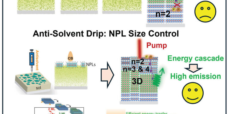
Graphical summary. Credit: Matter (2024). DOI: 10.1016/j.matt.2024.09.010
Researchers have developed and demonstrated a technique that allows them to engineer a class of materials called layered hybrid perovskites (LHPs) down to the atomic level, which precisely dictates how materials convert electrical charge into light. This technique opens the door to engineering materials suitable for use in next-generation printed LEDs and lasers and holds promise for engineering other materials for use in photovoltaic devices.
The article titled “Cationic Ligation Guides Quantum Well Formation in Layered Hybrid Perovskites” is published in the journal Matter.
Perovskites, defined by their crystal structure, possess sought-after optical, electronic and quantum properties. LHPs are made of incredibly thin sheets of perovskite semiconductor material that are separated from each other by thin organic “spacer” layers.
LHPs can be deposited as thin films consisting of multiple perovskite sheets and organic spacer layers. These materials are desirable because they can efficiently convert electrical charge into light, making them promising for use in next-generation LEDs, lasers, and photonic integrated circuits.
However, although LHPs have been of interest to the research community for years, it remains unclear how to design these materials to control their performance characteristics.
To understand what the researchers discovered, we need to start with quantum wells, which are sheets of semiconductor material sandwiched between spacer layers.
“We knew that quantum wells were forming in LHPs — those are the layers,” says Aram Amassian, corresponding author of a paper on the work and professor of materials science and engineering at UT State University. North Carolina.
And understanding the size distribution of quantum wells is important because energy flows from high-energy structures to low-energy structures at the molecular level.
“A quantum well that is two atoms thick has a higher energy than a quantum well that is five atoms thick,” says Kenan Gundogdu, co-author of the paper and professor of physics at NC State. “And for the energy to flow efficiently, you want to have quantum wells that are three to four atoms thick between the quantum wells that are two and five atoms thick. You basically want to have a gradual slope over which the energy can descend in a cascade.
“But people studying LHPs ran into an anomaly: the size distribution of quantum wells in an LHP sample that could be detected by X-ray diffraction would be different from the size distribution of quantum wells that could be detected by optical spectroscopy,” Amassian said. said.
“For example, diffraction could tell you that your quantum wells are two atoms thick and that there is a massive three-dimensional crystal,” says Amassian. “But spectroscopy could tell you that you have quantum wells that are two atoms, three atoms, and four atoms thick, as well as an overall 3D phase.
“So the first question we asked ourselves was: why do we see this fundamental disconnect between X-ray diffraction and optical spectroscopy? And our second question was: how can we control the size and distribution of quantum wells in the LHP?”
Through a series of experiments, the researchers discovered that there was a key player involved in answering both of these questions: nanoplatelets.
“Nanoplatelets are individual sheets of perovskite that form on the surface of the solution that we use to create LHPs,” explains Amassian. “We found that these nanoplatelets essentially serve as templates for the layered materials that form beneath them. So if the nanoplatelet is two atoms thick, the LHP underneath forms as a series of wells quantum two atoms thick.
“However, the nanoplatelets themselves are not stable, like the rest of the LHP material. Instead, the thickness of the nanoplatelets continues to grow, adding new layers of atoms over time. So when the nanoplatelet is three atoms thick, it forms three-atom quantum wells, etc. And, finally, the nanoplatelet becomes so thick that it becomes a three-dimensional crystal.
This discovery also resolved the long-standing anomaly regarding why X-ray diffraction and optical spectroscopy provided different results. Diffraction detects the stacking of sheets and therefore does not detect nanoplatelets, whereas optical spectroscopy detects isolated sheets.
“What’s exciting is that we found that we can essentially stop the growth of nanoplatelets in a controlled way, essentially by adjusting the size and distribution of quantum wells in LHP films,” says Amassian. “And by controlling the size and layout of the quantum wells, we can achieve excellent energy cascades, meaning the material is very efficient and fast at channeling charges and energy for laser and LED applications .”
When the researchers discovered that nanoplatelets played a crucial role in the formation of perovskite layers in LHPs, they decided to see if the nanoplatelets could be used to modify the structure and properties of other perovskite materials, such as perovskites used to convert light into electricity. in solar cells and other photovoltaic technologies.
“We found that nanoplatelets play a similar role in other perovskite materials and can be used to engineer these materials to enhance the desired structure, thereby improving their photovoltaic performance and stability,” explains co-author Milad Abolhasani of the article and professor of ALCOA. Chemical and biomolecular engineering at NC State.
The article was co-authored by Kasra Darabi, Fazel Bateni, Tonghui Wang, Laine Taussig and Nathan Woodward, all Ph.D. graduates of NC State; Mihirsinh Chauhan, Boyu Guo, Jiantao Wang, Dovletgeldi Seyitliyev, Masoud Ghasemi and Xiangbin Han, all of whom are postdoctoral researchers at NC State; Evgeny Danilov, director of NC State’s Kinetic Imaging and Spectroscopy Laboratory; Xiaotong Li, assistant professor of chemistry at NC State; and Ruipeng Li of Brookhaven National Laboratory.
More information:
Kasra Darabi et al, Cation ligation guides quantum well formation in layered hybrid perovskites, Matter (2024). DOI: 10.1016/j.matt.2024.09.010
Provided by North Carolina State University
Quote: Perovskite materials engineering at the atomic level paves the way for new lasers and LEDs (October 11, 2024) retrieved October 11, 2024 from
This document is subject to copyright. Apart from fair use for private study or research purposes, no part may be reproduced without written permission. The content is provided for informational purposes only.


