

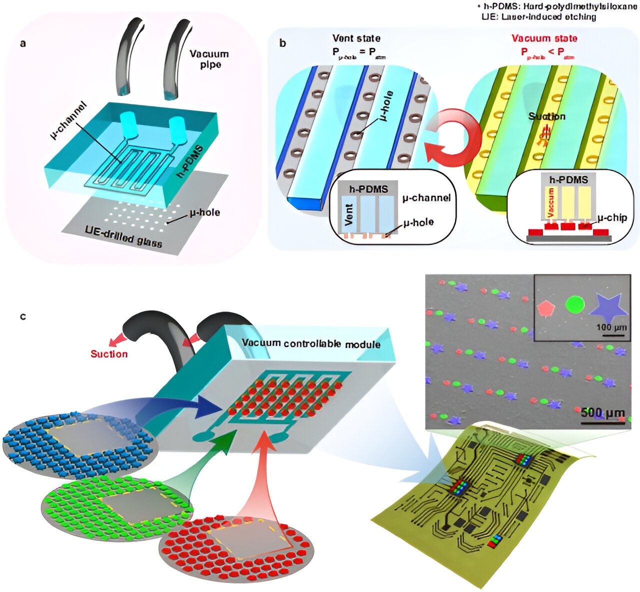
Concept of micro-vacuum assisted selective transfer printing (μVAST). Credit: Natural communications (2023). DOI: 10.1038/s41467-023-43342-8
A KAIST research team led by Professor Keon Jae Lee demonstrated transfer printing of a large number of micro-sized inorganic semiconductor chips via selective modulation of micro-vacuum force. The research, titled “Universal Printing by Selective Transfer via Micro-Vacuum Force,” is published in the journal Natural communications.
MicroLEDs are a light source for next-generation displays that use inorganic LED chips with a size of less than 100 μm. MicroLEDs have attracted much attention due to their superior electrical/optical properties, reliability and stability compared to conventional displays such as LCD, OLED and QD.
To commercialize microLEDs, transfer printing technology is essential to rearrange microLED arrays from a growth substrate onto the final substrate with a desired layout and precise alignment. However, previous transfer methods still had many challenges, such as the need for additional adhesives, misalignment, low transfer efficiency, and chip damage.
Professor Lee’s research team developed micro-vacuum-assisted selective transfer printing (µVAST) technology to transfer a large number of microLED chips by adjusting the suction force of the micro-vacuum.
The key technology relies on a laser-induced etching (LIE) method to form 20 µm micro-hole arrays with a high aspect ratio on glass substrates at a manufacturing speed of up to 7,000 holes per second. The LIE-drilled glass is connected to vacuum channels, controlling the strength of the micro-vacuum at the desired hole arrays to selectively capture and release the microLEDs.
Micro-vacuum-assisted transfer printing achieves higher adhesion switchability compared to previous transfer methods, enabling the assembly of micro-sized semiconductors with various heterogeneous materials, sizes, shapes and thicknesses on arbitrary substrates with high transfer efficiencies.
Professor Lee said: “Microvacuum-assisted transfer provides an attractive tool for large-scale selective integration of high-performance inorganic semiconductors at the micrometer scale. Currently, we are investigating transfer printing of commercial microLED chips with an ejection system for further commercialization. next generation displays (large screen TVs, flexible/expandable devices) and portable phototherapy patches.
More information:
Sang Hyun Park et al, Universal selective transfer printing via micro-vacuum force, Natural communications (2023). DOI: 10.1038/s41467-023-43342-8
Provided by Korea Advanced Institute of Science and Technology (KAIST)
Quote: Researchers develop selective transfer printing technology for microLEDs (December 19, 2023) retrieved December 19, 2023 from
This document is subject to copyright. Apart from fair use for private study or research purposes, no part may be reproduced without written permission. The content is provided for information only.
