

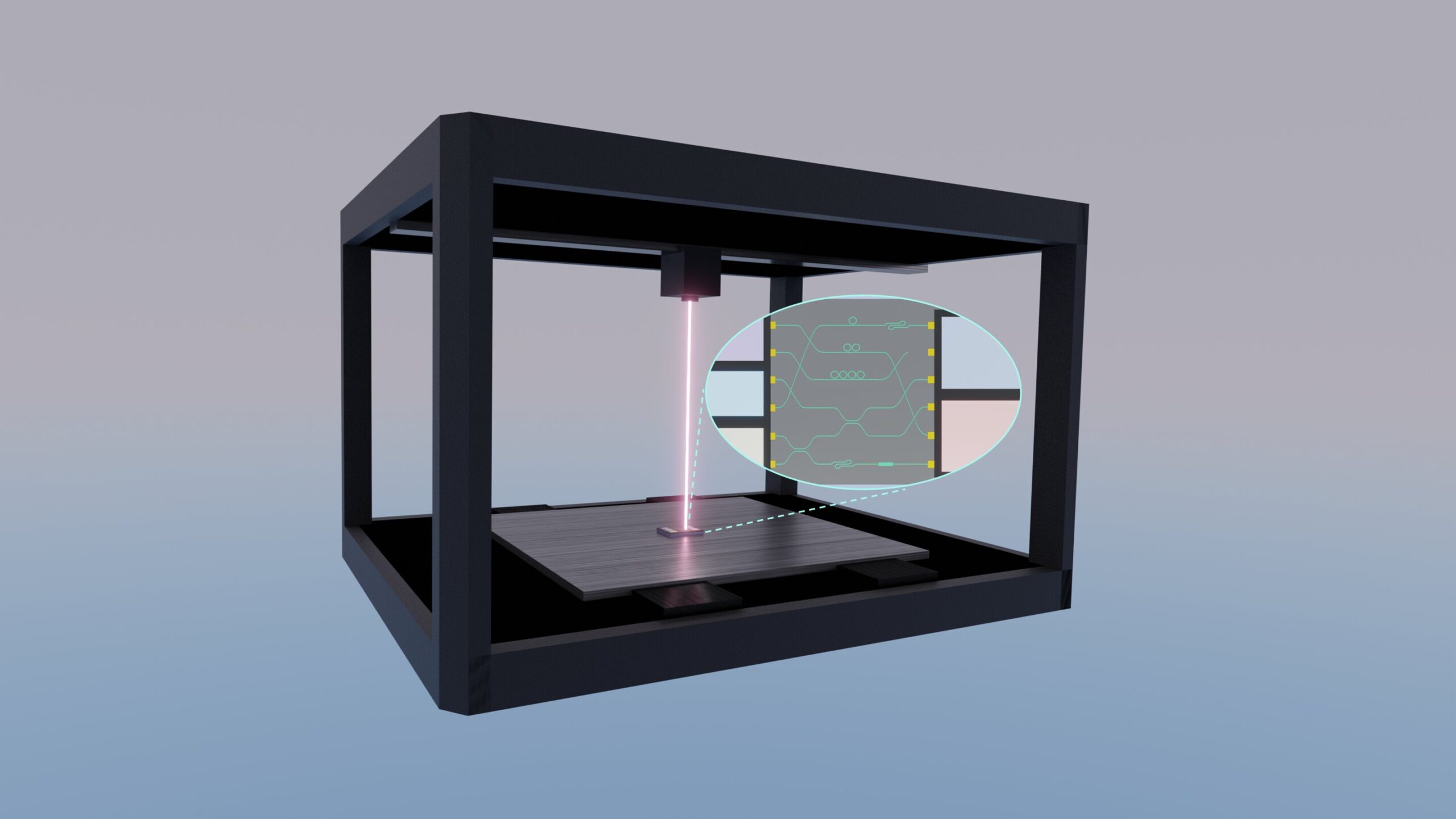
A research team led by Mo Li, a UW professor of electrical and computer engineering and physics, has invented a new way to print and reconfigure photonic integrated circuits (microchips) using a fast device and inexpensive in the size of a conventional desktop laser printer. This device could allow students and researchers to bypass costly nanofabrication facilities and produce photonic integrated circuits almost anywhere. The technology also has possible industrial applications. Credit: Haoquin Deng | University of Washington
Photonic integrated circuits are an important next-generation technology. These sophisticated microchips have the potential to significantly reduce costs and increase the speed and efficiency of electronic devices across a wide range of application areas, including automotive technology, communications, healthcare, data storage and data and computing for artificial intelligence.
Photonic circuits use photons, fundamental particles of light, to move, store and access information, much in the same way that conventional electronic circuits use electrons for this purpose. Photonic chips are already used today in advanced fiber optic communications systems, and they are being developed for implementation in a wide range of future technologies, including light detection and ranging, or LiDAR, for autonomous vehicles; light sensors for medical devices; 5G and 6G communications networks; and optical and quantum computing.
Given the wide range of existing and future uses for photonic integrated circuits, access to equipment capable of manufacturing chips for study, research and industrial applications is also important. However, today’s nanofabrication facilities cost millions of dollars to build and are well beyond the reach of many colleges, universities, and research laboratories.
For those who can access a nanofabrication facility, at least a day should be set aside for the demanding and time-consuming lithographic process used to make these microchips. Additionally, if an error is made in the design or the chip does not work properly for some other reason, the faulty circuit must be discarded, the design adjusted, and a new chip made. This often results in days or even weeks spent in a clean room.
But now, as described in a new article in Scientists progressA University of Washington-led research team has developed a way to bypass costly nanofabrication facilities and produce photonic integrated circuits almost anywhere.
The team developed an innovative method in which these circuits can be written, erased and modified by a laser engraver into a thin film of phase-change material similar to that used for recordable CDs and DVDs. This new process allows photonic integrated circuits to be built and reconfigured in a fraction of the time it would take in a nanofabrication lab.
The multi-academic team was led by Mo Li, UW professor of electrical and computer engineering and physics, associate chair for research in the department, member of the Institute for Nanoengineered Systems, and lead author of the article.
“Photonics technology is on the horizon; therefore, we need to train or educate our students in this area. But for students to study and gain hands-on experience with photonics circuits, they currently need access to a facility of several million dollars,” Li said.
“This new technology solves this problem. With our method, photonic circuits that previously had to be manufactured in expensive, hard-to-access facilities can now be printed and reconfigured in laboratories, classrooms and even garages, e.g. a quick and inexpensive way.-an expensive device the size of a conventional office laser printer.
Benefits for students, researchers and industry
Students aren’t the only ones to benefit from this new way of creating photonic integrated circuits. For researchers, this advancement will allow a much faster turnaround time to prototype and test a new idea before setting aside valuable time in a nanofabrication facility.
And for industrial applications, a big advantage of this method of producing photonic integrated circuits is reconfigurability. For example, companies could potentially use this technology to create reconfigurable optical connections in data centers, particularly in systems supporting artificial intelligence and machine learning, leading to cost savings and efficiency of production.
Li’s research team included UW ECE graduate student Changming Wu, lead author of the paper, and, along with Li, came up with the idea for this new way of building photonic integrated circuits. UW ECE graduate student Haoqin Deng also contributed to this effort. Their work is the latest result of a six-year line of research at the UW that includes advances in optical computing. It is also a continuation of a productive collaboration with Professors Ichiro Takeuchi and Carlos A. Ríos Ocampo and their students at the University of Maryland.
“Being able to write a complete photonic circuit in a single step, without a complicated manufacturing process, is really exciting. And the fact that we can make any modification to any part of the circuit in our own laboratory and rewriting it and redoing it is amazing,” Wu said. “It’s a matter of minutes instead of a whole day process. It’s a huge relief to be able to complete the entire manufacturing process in minutes instead of what often takes several days or even a week.”
Improve performance, build a commercial device
The method developed by the team has proven itself, but it is still an early-stage concept. However, Li has filed a provisional patent application and he plans to build a desktop laser engraver for photonic integrated circuits. This printer could be sold at an affordable price and widely distributed to research laboratories and educational institutions around the world. He also engages with industry leaders to promote possible applications of this new technology in programmable photonic chips and reconfigurable optical networks.
This laser printer for photonic chips will use a staging system that will move the substrate much more precisely than in a traditional desktop printer. The team will look for ways to optimize its performance when building a prototype. They will also work to reduce optical loss in the phase change material they use through further research into materials science and laser writing techniques. This will allow the printer to produce even more detailed and sophisticated circuits than is currently possible.
Li said he and his research team are very excited about what lies ahead.
“This technology can create the photonic circuits you want, but it can also be added to already existing electronic circuits. And because it is reconfigurable and reusable, it opens up many possibilities for students, researchers and industry,” said Li. “What excites me most is that we will potentially have a huge impact on the field of photonics by disseminating this new tool and technology to the entire research community.”
More information:
Changming Wu et al, Free-form direct-write and rewritable photonic integrated circuits in phase-change thin films, Scientists progress (2024). DOI: 10.1126/sciadv.adk1361
Provided by the University of Washington
Quote: The team develops a laser printer for photonic chips (February 1, 2024) retrieved February 1, 2024 from
This document is subject to copyright. Except for fair use for private study or research purposes, no part may be reproduced without written permission. The content is provided for information only.
